Bpsk Modulation And Demodulation Circuit Diagram What Is Pha
Block diagram of typical bpsk demodulation schemes using carrier Bpsk demodulation carrier recovery Bpsk modulation demodulation phase binary keying
Block diagram of typical BPSK demodulation schemes using carrier
Dpsk modulation,dpsk demodulation,differential phase shift keying Bpsk modulation and demodulation Bpsk block demodulation schemes carrier
Bpsk modulation & demodulation (matlab & python)
Bpsk demodulator. (a) circuit diagram. (b) waveform of each nodeBpsk modulation and demodulation Block diagram of typical bpsk demodulation schemes using carrierBpsk demodulation scheme.
Psk demodulation block diagramBpsk modulation demodulation transmitter matlab shift keying phase binary python gaussianwaves represented oscillator frequency multiplying running positive Block diagram of the proposed bpsk demodulation scheme.Bpsk modulation/demodulation topology..

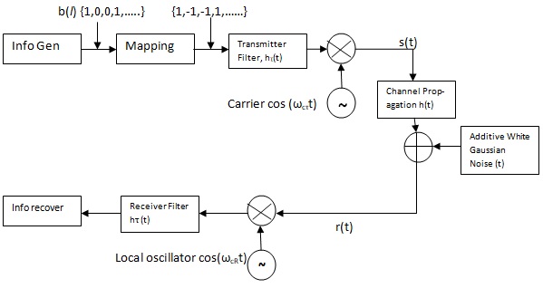
Bpsk modulation and demodulation
Bpsk demodulator circuit diagramBpsk modulation and demodulation circuit diagram Block diagram of bpsk demodulator v. result and discussion afterBlock diagram of typical bpsk demodulation schemes using carrier.
Bpsk diagram demodulation shift phase keying binary digital detector theory data experiment fig setBpsk modulation demodulation amplitude phasor carrier varactor ilo adding resulting recovery Bpsk demodulator circuit diagram4 schematic representation of normal bpsk modulation the left part.

Bpsk demodulation carrier recovery
Bpsk modulator-demodulatorDpsk demodulator demodulation differential phase shift keying modulation using rfwireless modulator world basics Figure 1. bpsk modulation and demodulation: (a) bpsk modulation processBinary phase shift keying (bpsk) modulation and demodulation technique.
Bpsk modulator |bpsk demodulatorFigure 1 from a cmos direct-digital bpsk modulator using an active Bpsk modulation and demodulation- complete matlab code with explanationBpsk modulation and demodulation circuit.

Bpsk modulation modulator demodulation matlab explanation implementation
Bpsk synchronous demodulation modulation phase figure constellations labBpsk demodulation modulation figure process pulse publishing education science figures index next Bpsk modulator circuitFigure 1 from design and implementation of bpsk modulator and.
What is phase shift keying (psk)? bpsk modulation, bpsk demodulationBpsk modulation and demodulation circuit diagram Bpsk demodulation modulationBpsk demodulator waveform.

Bpsk demodulation diagram block detection coherent signal phase psk modulation shift keying shown below
Phase shift keying modulation and demodulationBpsk modulation and demodulation Bpsk modulation demodulationBpsk modulation and demodulation circuit diagram.
Bpsk modulator cmosBlock diagram of typical bpsk demodulation schemes using carrier .